Welcome to the Precision Mechatronics Lab at the University of Newcastle
Conferences
IEEE International Conference On Mechatronics – Loughborough, UK, March 15-17, 2023
IEEE International Conference On Mechatronics - Loughborough, UK, March 15-17, 2023. IEEE International Conference on Mechatronics 2023 (IEEE ICM 2023) continues a series of biennial conferences dedicated to recent and [...]
Soft Robotic Manta Rays
PhD student Matheus Xavier introduces his research on soft robotic manta rays for low-impact exploration in sensitive underwater environments. Watch the video. https://youtu.be/BAN7ZxoomYo
News
Soft Robotic Manta Rays
PhD student Matheus Xavier introduces his research on soft robotic manta rays for low-impact exploration [...]

Dr Michael Ruppert elected as Fresh Scientist for 2021
Doctor Michael Ruppert has been announced as one of the 2021 Fresh Scientists. This program is [...]
Matheus Xavier Wins School Heat of the 3 Minute Thesis
Matheus from the Precision Mechatronics Lab wins the school heat at the University of Newcastle [...]
Double ARC Grants for the Precision Mechatronics Lab
The Precision Mechatronics Lab was successful in receiving a 2021 ARC DP and a 2021 ARC LIEF grant.
Seminars
Soft Robotic Manta Rays
PhD student Matheus Xavier introduces his research on soft robotic manta rays for low-impact exploration in sensitive underwater environments. Watch [...]
Dr Michael Ruppert elected as Fresh Scientist for 2021
Doctor Michael Ruppert has been announced as one of the 2021 Fresh Scientists. This program is run by Science in Public [...]
Matheus Xavier Wins School Heat of the 3 Minute Thesis
Matheus from the Precision Mechatronics Lab wins the school heat at the University of Newcastle of the 2021 3 Minute [...]
Double ARC Grants for the Precision Mechatronics Lab
The Precision Mechatronics Lab was successful in receiving a 2021 ARC DP and a 2021 ARC LIEF grant.
The Precision Mechatronics Lab develops new devices and processes for imaging and fabrication. This includes new sensors, actuators and control systems for applications in microscopy, mask-less lithography, and biomedical imaging.

The Precision Mechatronics Lab is supported by the Australian Research Council, Industrial Partners, The Center for Complex Dynamics Systems and Control (CDSC), and the University of Newcastle.

The University of Newcastle is ranked in the top 3% of world universities and #26 for a university under 50 years old. We are a research intensive university with a world-wide reputation for research in Engineering, the Sciences, and Medicine.
Recent Publications
Actuating, Sensing, Control, and Instrumentation for Ultra Precision Engineering Book
2024, ISBN: 978-3-0365-9526-9.

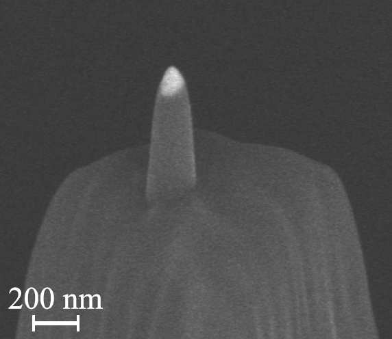
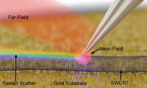
Feasibility of gold nanocones for collocated tip-enhanced Raman spectroscopy and atomic force microscope imaging Journal Article Forthcoming
In: Journal of Raman Spectroscopy, Forthcoming, ISSN: 1097-4555.
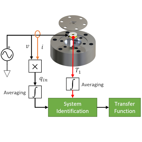
Thermal Protection of Piezoelectric Actuators Using Complex Electrical Power Measurements and Simplified Thermal Models Journal Article Forthcoming
In: IEEE/ASME Transactions on Mechatronics, Forthcoming, ISBN: 1083-4435.
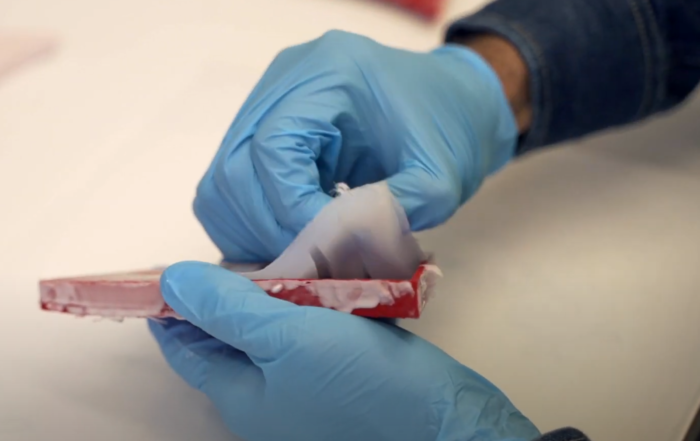
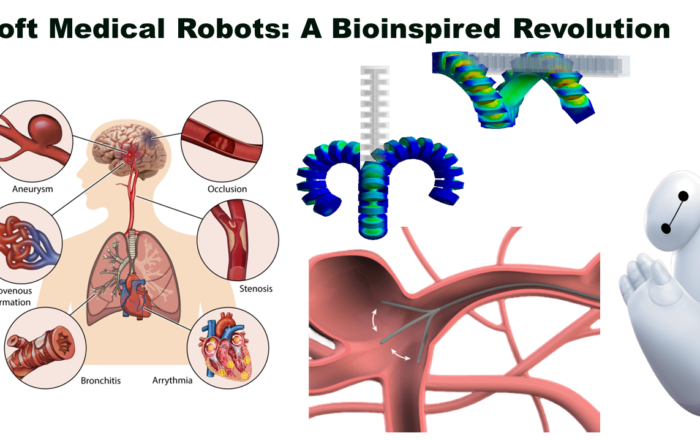
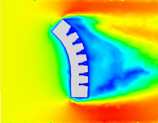
Modeling of soft fluidic actuators using fluid-structure interaction simulations with underwater applications Journal Article
In: International Journal of Mechanical Sciences, vol. 255, iss. 108437, pp. 1-11, 2023, ISSN: 1879-2162.
In: ACS Applied Nano Materials, vol. 5, iss. 7, pp. 9024-9033, 2022, ISSN: 2574-0970.
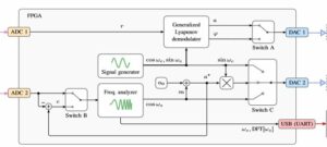
The Generalized Lyapunov Demodulator: High-Bandwidth, Low-Noise Amplitude and Phase Estimation Journal Article
In: IEEE Open Journal of Control Systems, 2022.